
What You'll Learn
Six core VLSI domains — from semiconductor physics and CMOS design to ASIC flows, physical design, and emerging chip technologies
Semiconductor Devices & Digital Logic
PN junctions, MOS capacitors, MOS transistors, Boolean algebra, combinational/sequential circuits, flip-flops, counters.
FoundationCMOS Logic Design
CMOS transistor operation, CMOS gates and circuits, timing diagrams, power analysis, and low-power design techniques.
Core SkillVLSI Design Methodologies
Design process, specifications, conceptual design, RTL coding, synthesis, layout design, verification, and testability.
In-DemandPhysical Design & ASIC Flow
Floorplanning, placement, routing, power distribution networks, front-end and back-end ASIC design flows.
AdvancedVerification, FPGA & Analog
Simulation, formal verification, test pattern generation, FPGA architecture and HDL programming, op-amp and data converter circuits.
Applied DesignDFM, SoC & Emerging Technologies
Design for Manufacturability, yield/reliability, SoC architecture, IP cores, nanometer CMOS, quantum and neuromorphic computing.
Cutting EdgeBuilt for the Chip Design Industry
A program spanning 13 modules — from semiconductor physics to SoC design — covering everything industry-aligned VLSI professionals need to know.
This course follows Skillumni's industry-aligned VLSI curriculum. You begin with strong foundations in semiconductor physics — intrinsic/extrinsic semiconductors, PN junctions, MOS capacitors, and MOS transistors. Then you build expertise in digital logic (Boolean algebra, combinational and sequential circuits) and CMOS design (gates, timing, power).
The course progresses through VLSI design methodologies including RTL coding, design synthesis, and layout, then advances to ASIC front-end and back-end flows, physical design (floorplanning, placement, routing, PDN), verification and testing, FPGA architecture and HDL programming, and analog circuit basics. The final modules cover DFM for yield enhancement, and advanced topics including SoC design, IP cores, nanometer CMOS, and emerging technologies like quantum and neuromorphic computing.
Course Benefits
Course Curriculum
Four stages, thirteen modules, one complete pathway from semiconductor physics to SoC and emerging chip technologies — click any module to expand
- Definition & history of VLSI
- Applications across industries
- Advantages of VLSI integration
- VLSI design hierarchy overview
- Intrinsic & extrinsic semiconductors
- PN junctions & diode operation
- MOS capacitors
- MOS transistors (NMOS & PMOS)
- Boolean algebra & minimization
- Logic gates & combinational circuits
- Sequential circuits & state machines
- Flip-flops, latches, counters, registers
- CMOS transistor operation
- CMOS logic gates & circuits
- CMOS timing diagrams
- CMOS design trade-offs
- VLSI design process overview
- Design specifications & requirements
- Conceptual design & RTL coding
- Design synthesis & layout
- Timing issues in digital circuits
- Power consumption in CMOS
- Design for Testability (DFT)
- Low-power design techniques
- Physical design overview
- Floorplanning & placement
- Routing & layout
- Power distribution networks (PDN)
- Intro to ASIC design
- ASIC design flow & methodologies
- Front-end design (RTL, synthesis)
- Back-end design (PnR, STA)
- Simulation & emulation
- Formal verification
- Test pattern generation
- Post-silicon validation
- FPGA architecture & configuration
- HDL programming for FPGAs
- Design tools for FPGAs
- FPGA vs ASIC trade-offs
- Intro to analog circuit design
- Op-amp circuits
- Filters & amplifiers
- Data converter circuits (ADC/DAC)
- DFM overview & importance
- Yield & reliability issues
- Layout optimization for yield
- Fault modeling & analysis
- System-on-Chip (SoC) design
- Intellectual Property (IP) cores
- Nanometer scale CMOS design
- Quantum & neuromorphic computing
Industry-Ready VLSI Engineer · Dual Certification · Placement Ready
13 modules stacked into a job-ready chip designer — from CMOS physics to SoC, backed by industry-aligned projects and a performance-based LOR.
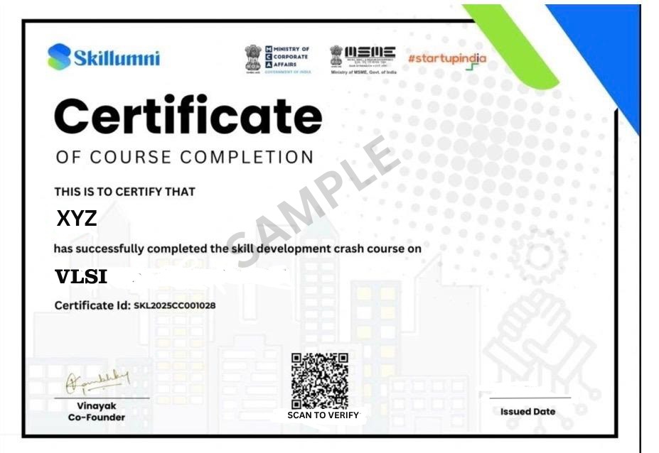
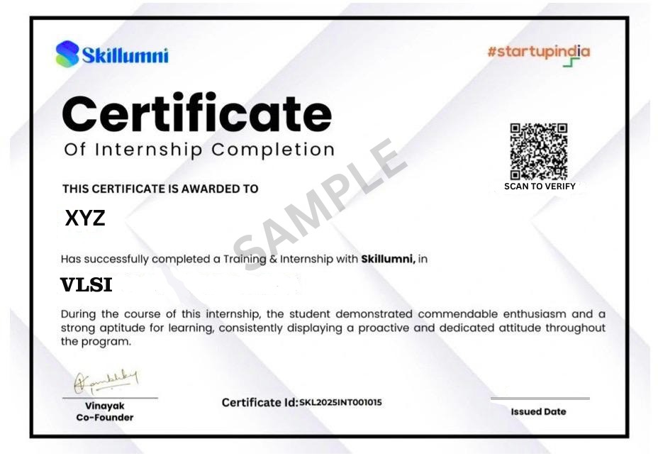
Your Dual Certificates
Two industry-recognized credentials awarded on successful completion
Why Choose This Course
Everything you need to launch a career in VLSI, ASIC, FPGA, or semiconductor design
Industry-Aligned Curriculum
Built on Skillumni's VLSI curriculum — from semiconductor devices and CMOS logic to ASIC flows, physical design, and SoC topics that semiconductor companies actually test.
Design-Flow Exercises
Apply VLSI concepts through logic design, timing analysis, RTL exercises, and guided case studies across ASIC, FPGA, and physical design workflows.
Dual Certification
Course Completion + Internship Certificate — credentials recognized by semiconductor companies, VLSI design houses, and EDA firms.
Performance-Based LOR
A star-rated, personalized Letter of Recommendation based on your actual work — differentiated proof of competence for chip design recruiters.
Expert Mentor Support
Direct access to VLSI and semiconductor professionals for doubt clearing, design reviews, and career guidance throughout the program.
Career & Placement Support
Placement assistance and referrals to our network of semiconductor companies, VLSI design firms, EDA companies, and product startups.
Requirements
- Basic digital electronics fundamentals (recommended)
- Interest in chip design, ASIC/FPGA, or VLSI careers
- Computer with internet connection
- Willingness to learn HDL concepts and VLSI design flows
Material Includes
- 35+ hours of video lectures by VLSI experts
- Lifetime LMS access — revisit anytime
- Section quizzes, assessments & exercises
- ASIC/FPGA design-flow case studies & projects
- Course Completion Certificate
- Internship Experience Certificate
Simple, Transparent Pricing
Pick the learning style that suits you best — both include dual certification and placement support